
Magnetron-sputtering Thin Film Deposition
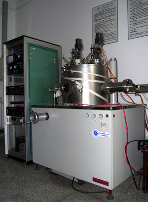
• Ultrahigh-vacuum chamber( 1x10⁻⁵Pa)
• Multilayer deposition with different targets
• Two DC and one RF electrical sources
• MAXTEK Film Deposition Controller (MDC-360)
• 0-300 V applied bias-voltage at substrate
Microwave Plasma Enhanced Chemical Vapor Deposition

• High-vacuum chamber( 3x10⁻⁴ Pa)
• Microwave power: 300-3000 W; Excitation frequency: 2.46 MHz
• Pressure range: 500-5000 Pa
• RT-1100 ℃ varied substrate temperature
• Four sets of gas flux controller
• 0-300 V applied bias-voltage at substrate
• Sample diameter: 100 mm
MML Nano-indenter
• Maximum Load: 500 mN
• Minimum Load: less than 1 uN
• Load Resolution: 30 nN
• Displacement Resolution: 0.001 nm
• Thermal-shift: ~0.004 nm/S
• X-Y Scope of In-situ Imaging:200 um x 200 um
Ultra-vacuum Electron Emission Measurement
• Ultrahigh-vacuum chamber( 6x10⁻⁸ Pa)
• Diode measurement configuration
• 0-10 keV DC applied voltage
• 0-5000 μm varied measurement distance
• LN-600 K varied measurement temperature
• Data automatically controlled and recorded by computer
TESCAN VEGA 3SB Scanning Electron Microscope

• Resolution: 3 nm at 30 kV;8 nm at 3 kV
• Magnification:4.5x-300,000x
• Accelerating Voltage: 200-30 kV DC
• Chamber Vacuum: < 9x10⁻³ Pa
• Image Size: Max 8192×8192, Rate of image size 1:1、4:3 or 2:1
Keithley 4200-SCS Semiconductor Characterization System
• Power Source: Vmax:200V;Imax:100 mA
• I-V Measurement:Voltage Resolution:1μV,Current Resolution:0.1 fA
• C-V Measurement: frequency range: 1 kHz ~10 MHz, Applied Voltage: 40 V
• Ultra-Fast I-V Measurement: Vmax 10V、Recommended minimum pulse width 20 nS
Electronic Film Stress Measuring Apparatus
• Sample size: 2~4 inch
• Min curvature: > 5m
• Precision: 5%
PARSTAT 2273 Advanced Potentiostat/Galvanostat

• Maximum Current: 2 A
• current resolution:1.2 fA
• Voltage range: 0-100 V
• Input Impedance: >1013 Ω
• Capacitance: <5 pF
• Frequence Range: 10 µHz - 1 MHz
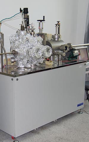
Magnetic-filtered Vacuum Arc Plasma Deposition
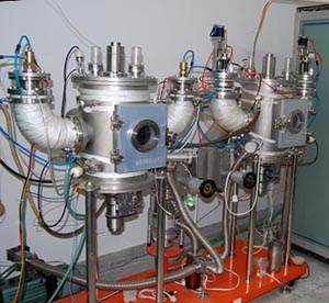
• High-vacuum chamber( 3x10⁻⁴ Pa)
• Two chambers configuration
• Multilayer deposition with different targets
• Ion Deposition with different ionized states
• 0-300 V applied bias-voltage at substrate
• Substrate Rotation with 0-30 r/min
Malven Zetasizer Nano ZS90
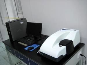
•Particle Size:0.3 nm - 5 μm
•Zeta Potential:No limitation
•Conductivity range:0-200mS/cm
•0-90 ℃ varied temperature
• Minimum volume: 12 μl
Thermo Fisher Biofuge stratos centrifuge
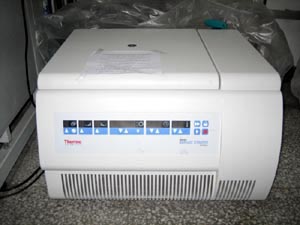
•Temperature range:-19℃-40℃
•Highest rotation rate:17000-23300rpm
•Largest centrifugal force:50377*g
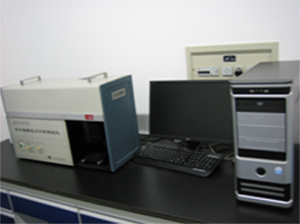
UV-Vis spectrometer
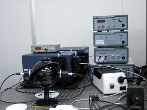
•Wavelength:200-2500 nm
•Resolution:0.1nm
•Spot size:Ф2~20mm
• Precision:1pA
Thermal Chemical Vapor Deposition
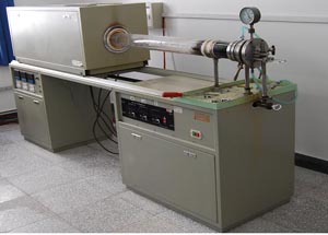
• Chamber: Ф100 mm quartz tube
• Working pressure: ambient pressure
• RT-1100 ℃ varied temperature
• Four sets of gas flux controller